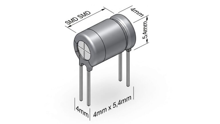
Choosing the right footprint for a surface‑mount electrolytic capacitor can make or break the performance, manufacturability, and service life of your printed circuit board. The smd 4 x 5.4mm electrolytic capacitor kicad model gives engineers a head start by combining accurate dimensions with KiCad‑ready symbol and footprint data, ensuring that virtual designs translate cleanly to real‑world assemblies.
Why Footprint Accuracy Matters for SMT Capacitors
Every SMT electrolytic capacitor has strict tolerances for pad size, solder mask expansion, and keep‑out distance. Undersized pads can impede solder wetting, while oversizing leads to tombstoning or excess paste. With compact power‑management designs trending toward higher current density, thermal dissipation and mechanical stability become critical factors. An exact KiCad model eliminates guesswork, saving costly board spins and assembly delays.
Designers working on IoT sensors, LED drivers, or buck converters often juggle space constraints against reliability targets. A well‑sized footprint ensures the ESR and ripple‑current ratings published by the capacitor vendor are achievable in practice, not just on paper.
Breaking Down the 4 × 5.4 mm Electrolytic Package Dimensions
The 4 × 5.4 mm format is popular in wearables, drones, and other portable devices where height restrictions are tight. Despite its small stature, the package must house a wound foil, electrolyte, and rubber seal without compromising voltage capability or lifetime.
Matching Real‑World Parts to ECAD Data
Before dropping a generic footprint into your PCB layout, cross‑check the manufacturer’s datasheet for land pattern recommendations. Minor variations—such as can diameter tolerance or lead‑frame length—can shift the centerline. By aligning those numbers with the smd 4 x 5.4mm electrolytic capacitor kicad model, you lock in true‑to‑spec clearances for pick‑and‑place machines and automated optical inspection.
Creating and Importing the KiCad Library Entry
Although KiCad’s default libraries cover many components, niche electrolytics often require custom entries. Start in the Footprint Editor and set the courtyard outline 0.25 mm beyond the pad edges to satisfy IPC‑7351B guidelines. Define rounded‑rect pads for improved solder‑joint filleting, and remember to assign the polarity marker to Pad 1 for unambiguous assembly references.
Once the footprint is complete, export it to a dedicated library folder. Next, generate the schematic symbol, map the positive and negative pins, and link the symbol to your new footprint. When you add the smd 4 x 5.4mm electrolytic capacitor kicad model to a schematic, the 3D viewer instantly displays a lifelike can rendered at 1:1 scale—perfect for clearance checks in crowded enclosures.
Step‑by‑Step Footprint Generation
- Create two circular or oval pads 1.2 mm in diameter, spaced 2.0 mm apart.
- Add a silkscreen polarity stripe adjacent to the negative lead.
- Draw a 0.05 mm courtyard layer outline.
- Specify a 3D model reference (.wrl or .step) for realistic visualization.
- Save and test the footprint on a demo board before deploying it company‑wide.
Common Pitfalls and How to Avoid Them
Even seasoned engineers can stumble over simple mistakes:
- Misaligned polarity: Double‑check that Pad 1 aligns with the positive can marking in both the schematic and PCB views.
- Via in pad: While tempting for heat sinking, vias in electrolytic pads risk wicking solder and starving the joint. Offset them by at least 0.3 mm.
- Excess solder paste: For tiny cans, stencil apertures should be reduced 10–15 % to curb slumping and bridging.
By verifying each detail against the smd 4 x 5.4mm electrolytic capacitor kicad model, you dramatically boost first‑pass yield and minimize field returns due to premature capacitor failure.
Testing and Validation in Prototype Assemblies
Once boards arrive from the fab, subject them to temperature cycling and power‑on hours to confirm capacitor stability. ESR drift, leakage current, and physical swelling are early indicators of stress. Capture thermal images to ensure nearby hot components don’t push core temperature beyond 105 °C, the typical ceiling for polymer electrolytics in this size class.
During functional testing, log voltage ripple across the rails at different load steps. The correct footprint should keep ESL low, letting the cap absorb transient spikes without overshoot. If measured performance deviates from simulations, re‑examine pad geometry, solder fillet height, and assembly profile.
Frequently Asked Questions
Q: Why can’t I reuse a 4 × 5 mm footprint from another project?
A: The extra 0.4 mm height and vendor‑specific lead‑frame geometry may cause polarity misalignment or insufficient paste coverage. Always validate against the latest datasheet.
Q: Does the KiCad model include a 3D STEP file?
A: Yes. Importing the STEP file allows accurate mechanical collision checks within enclosure CAD tools.
Q: How do I handle derating for voltage and temperature?
A: Keep operating voltage below 80 % of the rated value, and ensure ambient plus self‑heating stays at least 10 °C under the stated maximum.
Q: Can I mirror the footprint for the board’s bottom side?
A: Mirroring is safe if polarity markers remain clear; update silkscreen and assembly notes accordingly.
Q: What stencil thickness works best?
A: A 0.1 mm (4 mil) stainless stencil with reduced aperture size balances solder volume and wetting.
Conclusion
Mastering the smd 4 x 5.4mm electrolytic capacitor kicad model is more than a library exercise—it’s a gateway to reliable, compact, and manufacturable electronics. By paying close attention to footprint accuracy, polarity marking, and thermal considerations, you ensure that your boards perform in the lab and thrive in the field. With a solid KiCad model in place, your next power‑supply or sensor design will be one step closer to first‑time‑right success.

